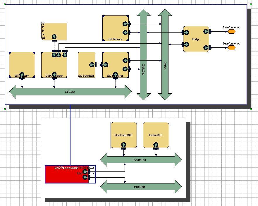
Creating the initial model for the platform was quite straightforward. Taking the description and diagrams from the SH2 platform manual the initial VCC model structure of the SH2 was quite obvious and easy to build. This initial model can be seen below in Fig. 3.
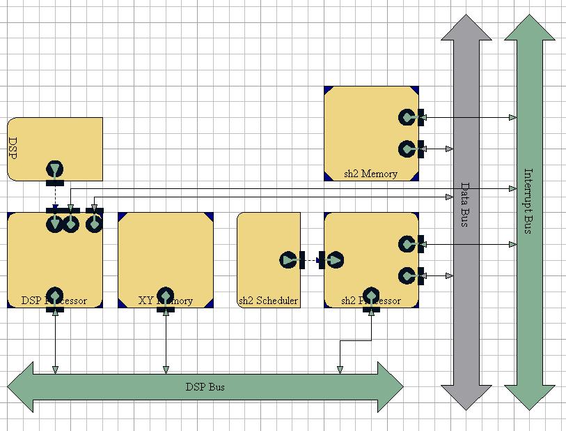
It can be seen that the model consists of several major components. From the top left we can see the DSP Scheduler, which is essentially a Real-Time Operating System (RTOS) that is used to schedule processes to be calculated by the processor, located immediately below the scheduler. This in turn is connected to the DSP bus, a special bus connecting one of the SH2DSP memory areas and the main SH2 processor. Accordingly, the XY memory and the SH2 processor, along with its associated scheduler can be seen attached to the DSP bus. The other two buses are the main system data bus and an interrupt bus. The data bus also connects to the main SH2DSP system memory.
This model was used for testing of several different implementations of the application and the Bluetooth stack behaviours. These tests and their associated results are detailed in the CARMA application and Bluetooth stack portions of this report.
It was later discovered, however, that this initial model was not fully suitable for the purpose of the project. We were going to need to add the possibility of an ASIC for both testing purposes while building the mappings and also to act as a hardware ASIC possibility for parts of the application.
Under normal circumstances any external devices to the SH2 would be attached to the data bus. It would be easy to attach a device to this directly, however it is probably a better idea to generalise the model of the SH2 processing platform down to a single VCC block so that it can be used in future projects directly. This can be done by making a few changes to the model and then generating a new symbol for it. Firstly, a new ASIC was added to the model, attached to the data and interrupt buses. An external input and output port were then also attached to the ASIC. A new symbol representing the entire processor architecture could then be generated. When it comes to mapping behaviours to the model we can now map a simple input -> output behaviour to the new ASIC, which acts as a bridge device. The architecture being attached-to can now be given data and interrupt buses as if they were directly connected to the SH2 processor platform. The new model and also its representative block is shown in Figs 4 and 5 below.